LVBMS
The LVBMS monitors the car's low-voltage battery the way the rules-mandated BMS watches the high-voltage accumulator, except nothing requires this board to exist. It reads per-cell voltage on every series cell of the 12S3P pack, cell temperature through NTC thermistors, and pack current through a hall-effect sensor, and hands all of it to the vehicle's critical CAN bus.
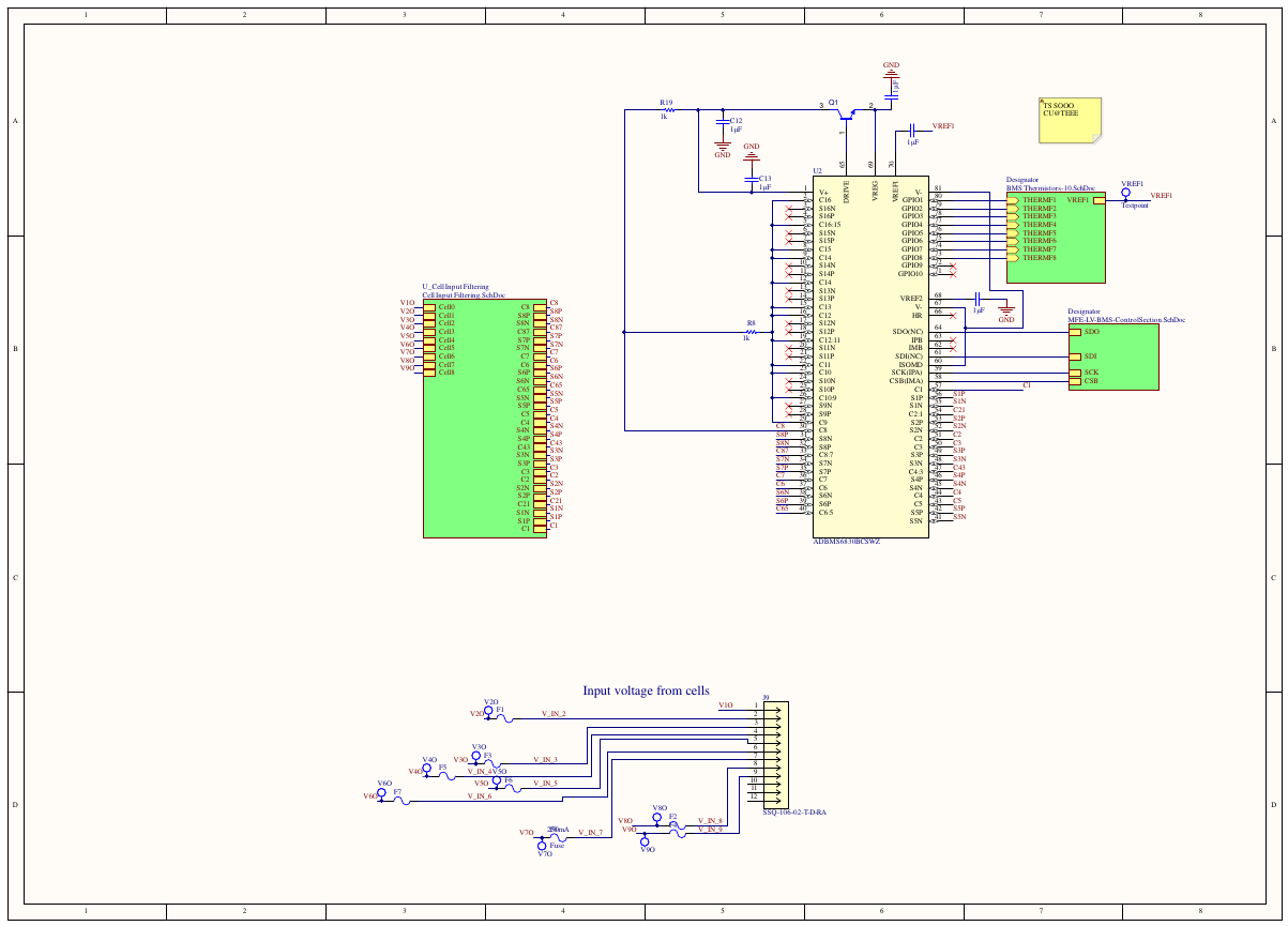
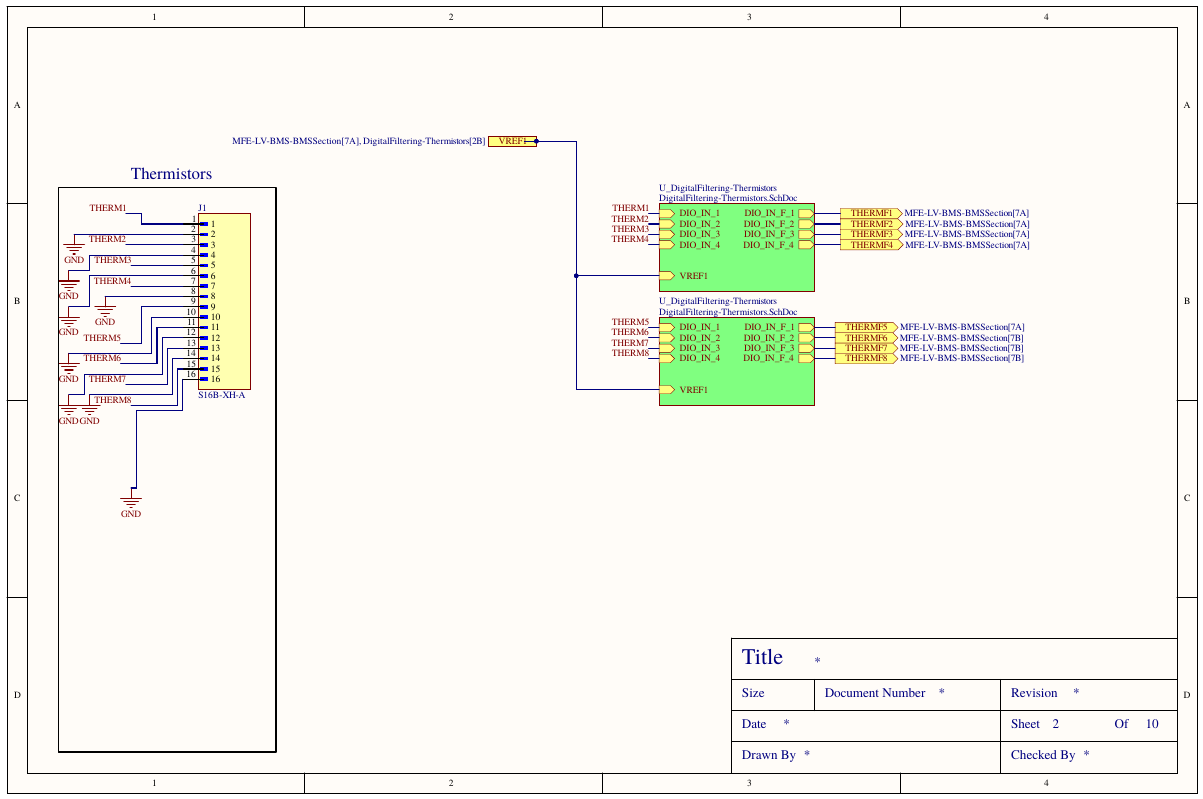
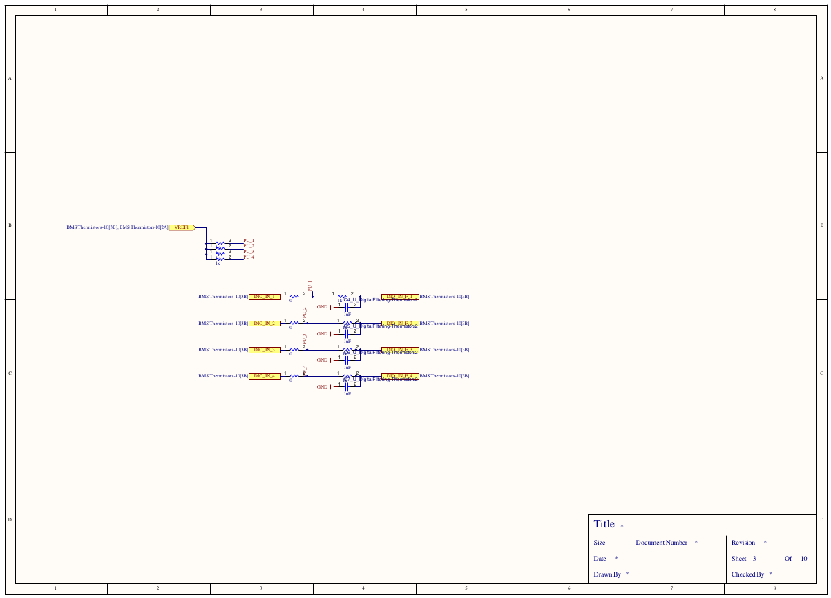
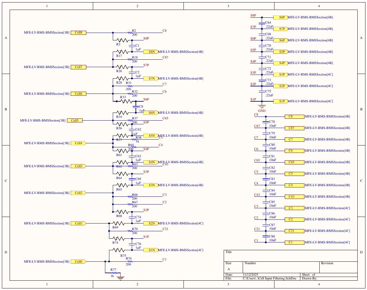
Each series cell tap runs through an RC filter before the monitor IC, which measures cells in overlapping sets of three (cell n, the n/n−1 junction, cell n−1). Balancing is passive: the chip switches in bleed resistors on any cell sitting above the lowest cell's potential, discharging the pack into equilibrium from the top down. Thermistor taps are RC-filtered and referenced to VREF1 (5V).
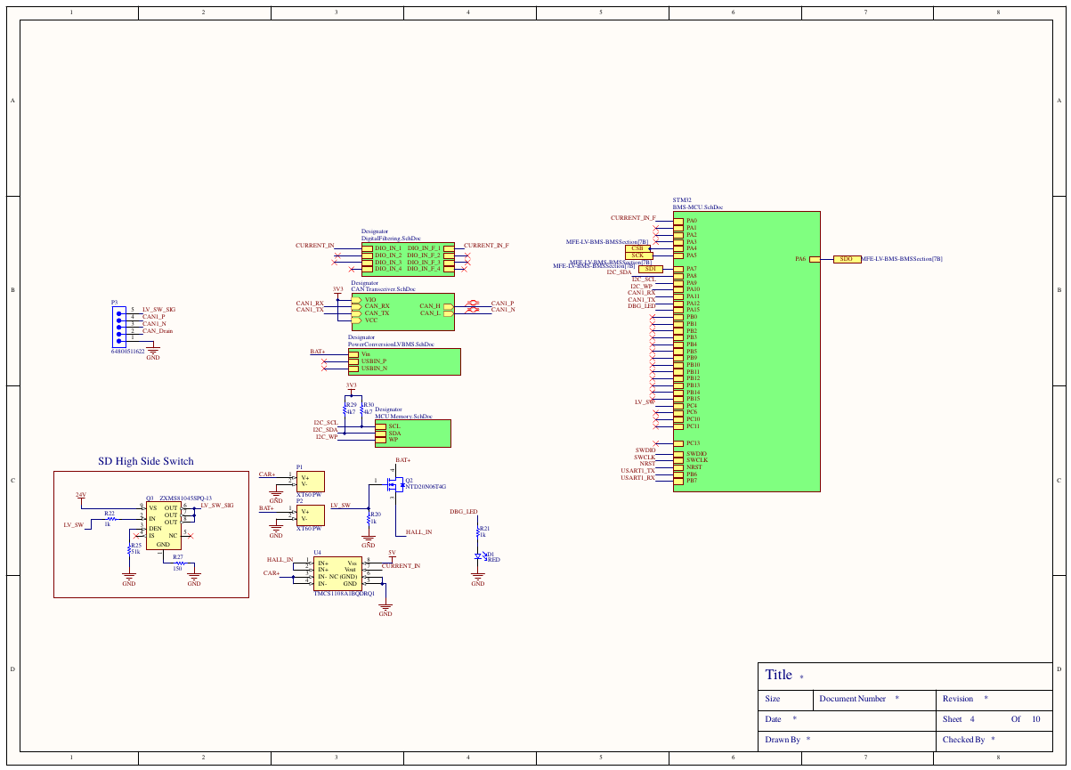
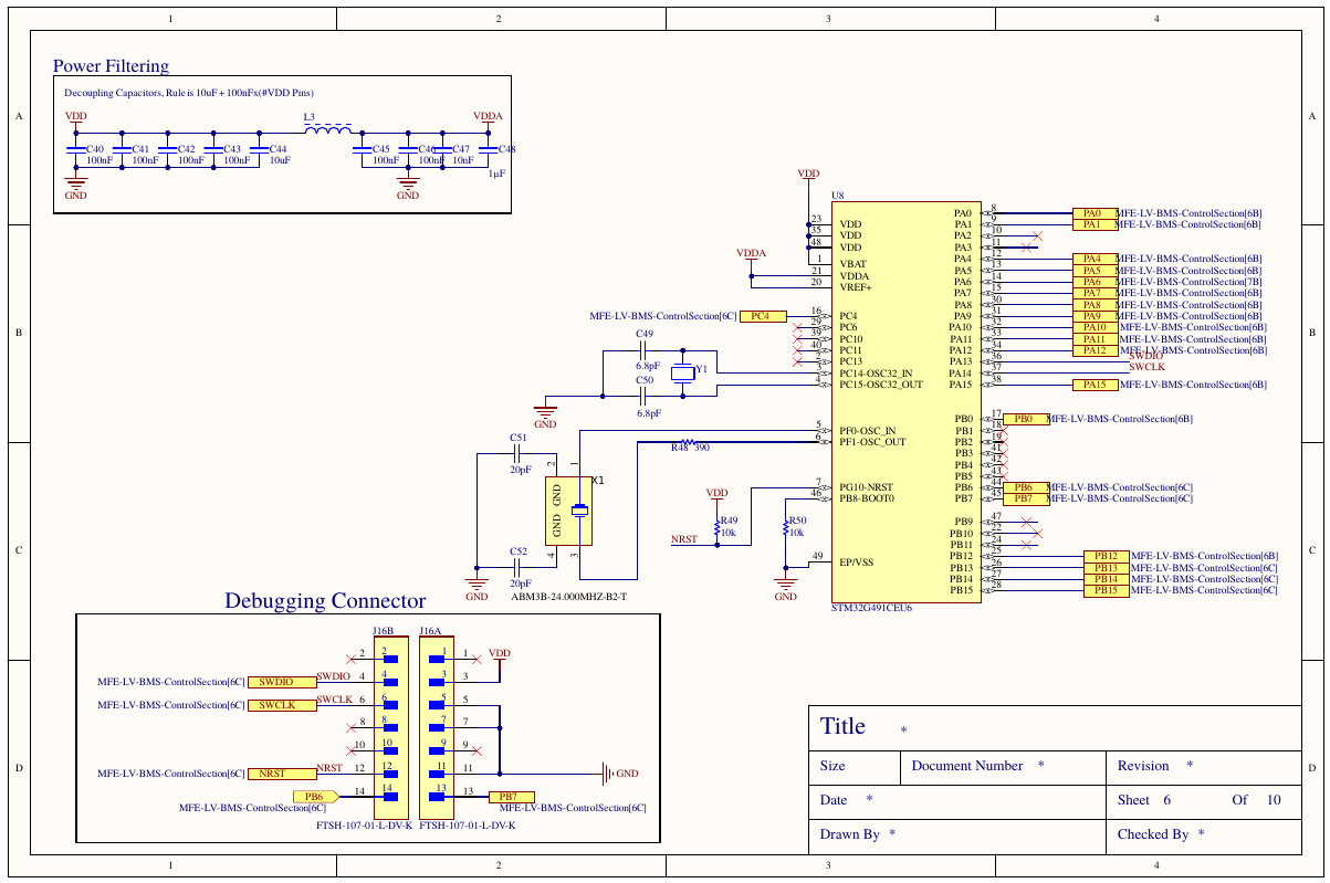
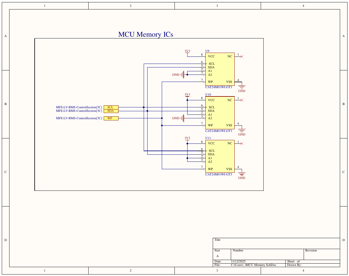
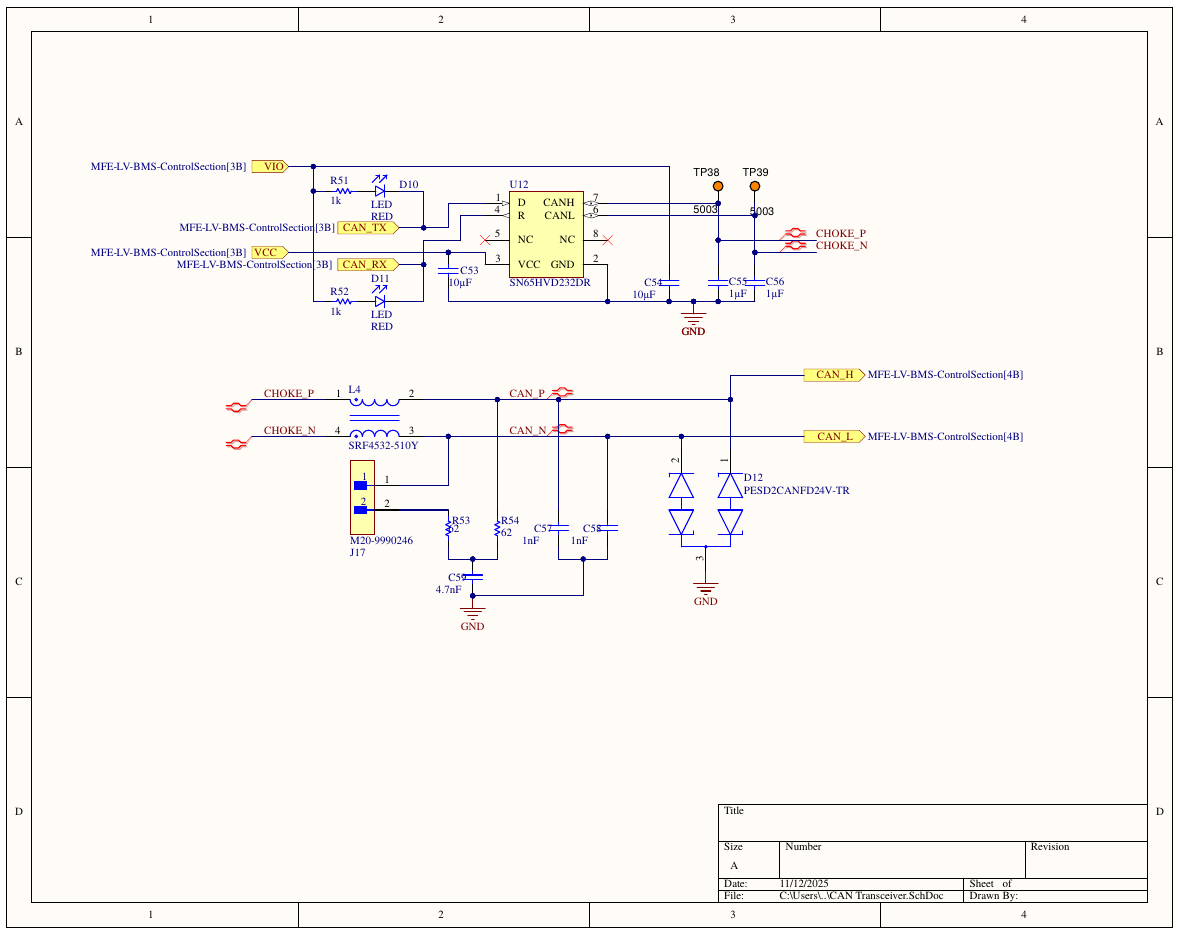
The monitor IC talks SPI to an STM32, an architecture switch I led from the previous UART design, for modularity. The MCU publishes to critical CAN through a transceiver that converts the STM32's RX/TX into the CANP/CANN differential pair, logs to I²C memory ICs, and exposes UART for debug. Q2 is a software-controlled battery disconnect: the MCU's LV_SW line connects or isolates the pack from the rest of the car.
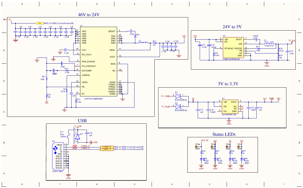
~30V from the LV pack steps down to 24V through a switching regulator with UVLO protection, then 24V → 5V → 3.3V for logic.
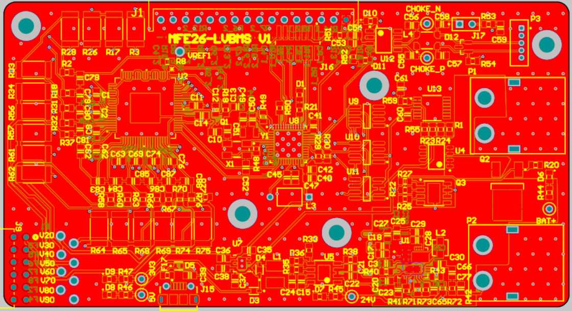
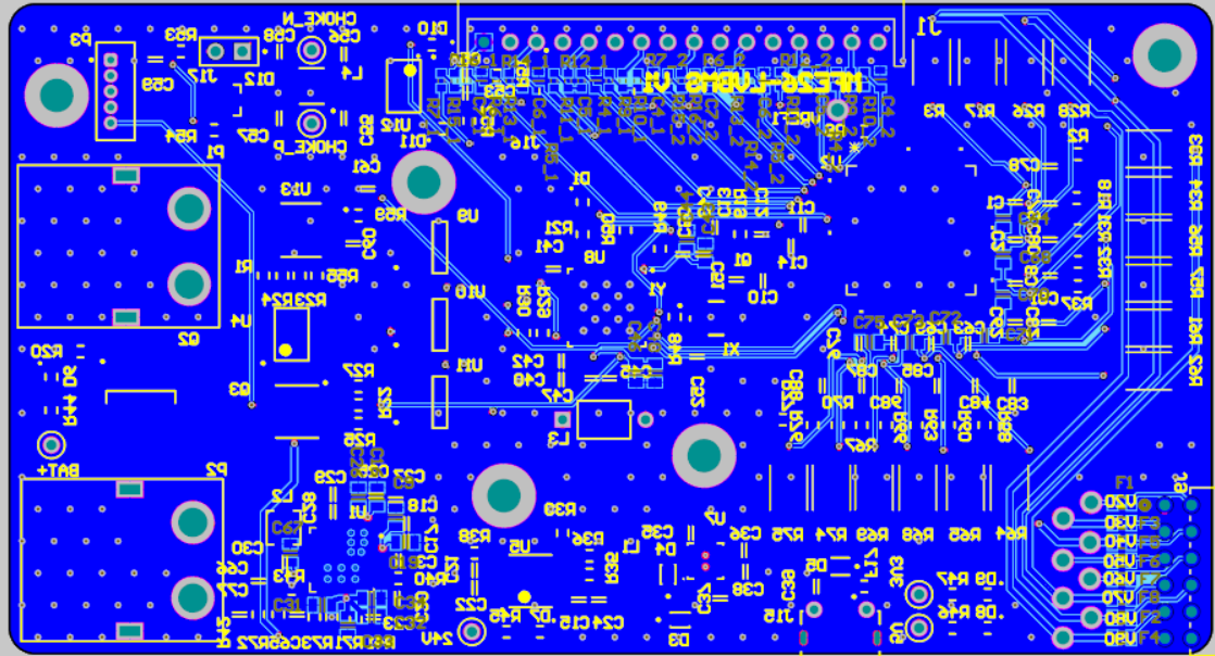
Four-layer stackup with dedicated internal planes: each mid layer pours as a single unbroken island, so outer-layer routing never breaks a return path. Cell-tap test points (V20–V90), rail test points (24V, 5V, 3V3, BAT+), and choke nodes are all brought out and labeled for bring-up.
Hierarchical design, ten sheets. The ADBMS6830 monitor reads the series cells of the 12S3P pack through the RC-filtered cell-input sheet, thermistors come in through their own filtering blocks off VREF1, and the control section ties the STM32G491 to the hall sensor (TMCS1108), CAN transceiver (SN65HVD232 with common-mode choke and ESD clamp), I²C EEPROM bank, and the LV_SW high-side disconnect. Power runs pack input → 24V (LM706A, UVLO) → 5V (LMR38020) → 3.3V (LD39050).

Design complete, fab pending. Bring-up plan once boards are back: verify the power tree rail by rail (24V, 5V, 3.3V), establish the SPI link to the monitor IC, then run a full cell-tap and balancing characterization against a bench supply before the board ever touches the real pack. The main architecture change this revision was moving the monitor interface from UART to SPI, which decoupled the cell-monitoring chain from the MCU's serial layout.